| |
Ge,N-type ,Sb & As -doped
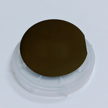
Ge Wafer (110) 4" dia x 0.5 mm,2SP, N type ( Sb doped) R:0.1-0.5ohm.cm
Ge Wafer Specification
• Growing Method: CZ • Orientation: (110) +/-0.5 Deg.
Major Flat: <111>
• Wafer Size: 4" dia x 500 microns • Surface Polishing: two sides epi polished • Surface roughness: < 30 A ( by AFM) • Doping: Sb Doped • Conductor type: N-type • EPD: <100 /cm^2 • Package: under 1000 class clean room
Typical Properties of Ge Crystal
- • Structure: Cubic, a = 5.6754 A
- • Density: 5.323 g/cm3 at room temperature
- • Melting Point: 937.4 oC
- • Thermal Conductivity: 640
|