| |
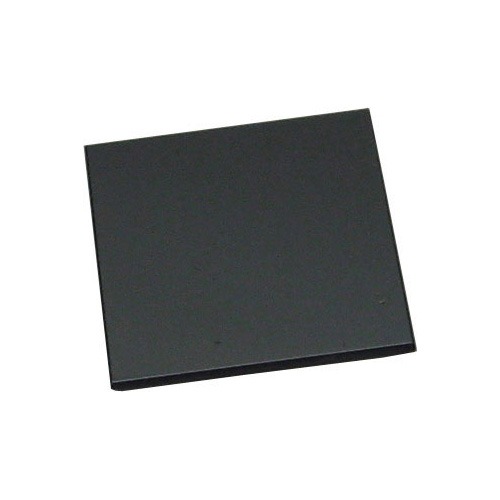
SOI Wafer ( Silicon On Insulator )
SOI Wafer:5x5x0.625mm, 2 .5µm (P-doped) +1.0 SiO2 +625um Si (P-type /Boron doped)
Specifications
Device Layer
| Size: | | 5mmx5mm | Type/Dopant: | | N type/P-doped | Orientation: | | <1-0-0>+/-0.5 degree | Thickness: | | 2.5±0.5µm
| Resistivity: | | 1-4 ohm-cm | Finish: | | Front Side Polished | Buried Thermal Oxide:
| Thickness: | | 1.0 um +/- 0.1 um | Handle Wafers:
| Type/Dopant | | P type/B-doped | Orientation | | <1-0-0>+/-0.5 degree | Resistivity: | | 10-20 ohm.cm | Thickness: | | 625 +/- 15 um | Finish: | | As received (not polished) |
|