| |
Ge P-type Ga-doped
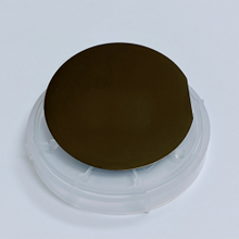
VGF-Ge Wafer(100), 100mm dia x 0.4 mm, 2SP, P type (Ga doped), R:0.0038-0.0158 Ohm.cm
Ge Wafer Specification
• Growing Method: VGF • Orientation: (100) +/-0.4 Deg. • Wafer Size: 100mm dia x 400 microns • Surface Polishing: Two sides polished • Surface roughness: < 8 A ( by AFM) • Doping: Ga Doped • Conductor type: P-type
Carrier Concentration: (0.64-6.67) x10^18 /c.c
EPD: <500 /cm
• Ra(Average Roughness) : < 0.4 nm • Package: under 1000 class clean room
Typical Properties of Ge Crystal
- • Structure: Cubic, a = 5.6754 A
- • Density: 5.323 g/cm3 at room temperature
- • Melting Point: 937.4 oC
- • Thermal Conductivity: 640
|
|
|

Working days : Monday to Saturday

|
|
|