GaN Template on saphhire is made by a hydride vapor phase epitaxy (HVPE)-based method. During the HVPE process, HCl reacts with molten Ga to form GaCl, which in turn reacts with NH3 to form GaN. GaN template is a cost effective way to replace GaN single crystal substrate.
Specifications
• Semi-Insulting GaN Epitaxial Template on Sapphire (C plane)
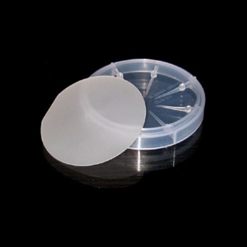
• Sizes: 3” Round
• Substrate Sapphire, Orientation c-axis (0001) +/- 1.0 o
• Conduction Type: n-type,undoped
• Typical Macro Defect Density:< 5cm-2
• Resistivity:>10^6 Ohm-cm
• Front Surface Finish (Ga Face) As-grown
• Back Surface Finish Sapphire as-received finish
• Useable Surface Area >90%
• Edge Exclusion Area 1mm
Typical Macro defect Density: <5cm^-2
• Package Single Wafer Container
• GaN layer thickness 5 microns , (+/- 10%) with roughness: ~10 nm RMS as measured by the Wyko (white light interferometer) for 50 umx50um area