| |
New Crystal
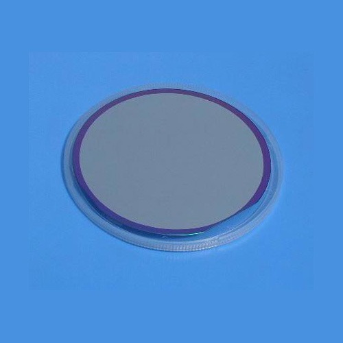
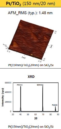
SiO2+TiO2+Pt(111) thin film on Si substrate ,4"x0.525mm,1sp P-type B-doped, (SiO2=300nm,TiO2=20nm ,Pt(111)=150nm)
- Silicon Wafer Specifications
- Resistivity
- 1 - 10 ohm.cm
- Substrate Size
- 4" diameter +/- 0.5 mm x 0.525 mm
- Surface roughness
- < 20 A RMS
- Maximum Thermal Budget of Pt film
- 800 - 900 degree C
- Optional
- you may need tool below to handle the wafer
( click picture to order )
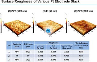
- Surface Roughness of Various Pt Electrode Stack
|
|
|

Working days : Monday to Saturday

|
|
|