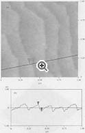
Step STO substrate is a atomically smooth SrTiO3 (100) with steps one unit cell in height was obtained by treating the crystal surface with a pH-controlled NH4F-HF solution. The homoepitaxy of SrTiO3 film on the crystal surface proceeds in a perfect layer-by-layer mode as verified by reflection high-energy electron diffraction and atomic force microscopy. Ion scattering spectroscopy revealed that the TiO2 atomic plane terminated the as-treated clean surface and that the terminating atomic layer could be tuned to the SrO atomic plane by homooepitaxial growth. This technology provides a well-defined substrate surface for atomically regulated epitaxial growth of such perovskite oxide films . For more information on Step substrate, please refer to the article at Science 2 December 1994:Vol. 266 no. 5190 pp. 1540-1542DOI: 10.1126/science.266.5190.1540
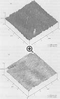
Surface of SrTiO3 substrate after Step treatment (AFM)
Surface of SrTiO3 substrate before Step treatment (AFM)
Typical AFM picture of step STO substrate
Substrate Specifications
Size
10 x 10 x 0.5 mm +/-0.05 mm
Orientation
0.1º miscut from (100) ( +/- 0.1º from Y and X direction )
Polish
One sides EPI polished by CMP tecnology with less sub-surface lattice damage
Surface Termination
TiO2 layer ( via special etching )
Surface finish (RMS or Ra)
< 5A
Manufactuer
Made in Japan
Typical Physical Properties
Crystal Structure
•Cubic, •a = 3.905 Å
Growth Method
Vernuil
Density
5.175 g/cm3
Melt Point
2080 oC
Hardness
6 ( Mohn )
Thermal expansion
10.4 (x10-6/ oC)
Dielectric Constant
~ 300
Loss Tangent at 10 GHz
•~ 5 x 10⁻⁴ @ 300 K , •~ 3 x 10⁻⁴ @ 77 K
Color and Appearance
Transparent (sometimes slightly brown based on annealing condition). No twins.