YBCO Epi. Film on SrTiO3 or LaAlO3

Au (300-400nm) Film on YBCO (500nm ) Template/ ( Two sides ) on LaAlO3, 2" dia.x0.5 mm,2spAu Film on YBCO TemplateYBCO(500nm)/LAO-50D05C2

Au (300-400nm) Film on YBCO (500nm ) Template/ ( Two sides ) on LaAlO3, 2" dia.x0.5 mm,2sp
Au Film on YBCO TemplateYBCO(500nm)/LAO-50D05C2

기본 정보
Product Name Au (300-400nm) Film on YBCO (500nm ) Template/ ( Two sides ) on LaAlO3, 2" dia.x0.5 mm,2sp
Au Film on YBCO TemplateYBCO(500nm)/LAO-50D05C2
Sale Price Call for Price
Product Code Au Film on YBCO...
Quantity 수량증가수량감소
상품 옵션
 
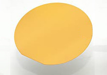
Item Number : Au Film on YBCO TemplateYBCO(500nm)/LAO-50D05C2
  • MTI Corp joins with several research institutes around the world, to finally make high Tc superconducting epitaxial thin film commercially available at an affordable price.    MTI supplies high quality double side epitaxial thin film up to 3" diameter on LaAlO3, LSAT, Al2O3 and SrTiO3 single crystal substrate by a unique technology.

    This will make YBCO thin film available at very low cost.     Researchers don't need to grow thin film any more, but concentrate their talent on HTSC film related devices, such as microwave filter for wireless and HTSC Squid.
  •  Silicon Wafer Specifications
  • Film
  • Au (300-400nm) Deposition on both sides on YBCO (500nm ) Template/ ( Two sides ) on LaAlO3

    ○  Au = 300-400 nm
    ○  YBCO = 500 nm

  • Substrates
  • YBCO ( 500 nm ) Template/ ( Two sides ) on LaAlO3
  • Substrate Size
  • 2" diameter +/- 0.5 mm x 0.5 mm
  • Polish
  • Two sides polished
  • Surface roughness Ra or RMS
  • < 5A
  • Optional
  • you may need tool below to handle the wafer ( click picture to order )
  •  Main Specifications of HTS Film
  • Epitaxial thin Film Composition
  • <100> YBCO
  • Film dimension
    both for one side
    or double side film
  • YBCO / LaAlO3 10x10 mm ~ 3" dia.
    YBCO / LSAT 10x10 mm ~ 2" dia.
    YBCO / Al2O3 10x10 mm ~3" dia
    YBCO / STO 10x10 mm ~ 1" dia.
  • Epitaxial FWHM
  • < 0.2 o
  • Critical Transition
    Temperature Tc
  • > 90 K
  • Transition Temp. range ΔTc
  • < 0.5 K
  • Critical Current Jc
  • 2~3 MA/cm2 @ 77K 0T
  • Surface Resistivity Rs
  • < 1 m Ohm @ 10 GHz,
    77K,
    0T
  • Thin film thickness
  • 200 ~ 500 nm upon request ,
  • Uniformity for 2" wafer
  • Thickness 400 nm +/- 10 %
    Tc 90K +/- 1 o
    Jc 3 +/-0.5 MA/cm2 @ 80% wafer center.
  • Package
  • Sealed in Vacuum in a plastic box and bag.

  • Double side 3" YBCO film on LaAlO3 Jc Uniformity measured FZK

  • XRD pattern of Epi YSCO Film on LAO
  • Note
  • YBCO is very sensitive to moisture, and must be stored in desiccator box.