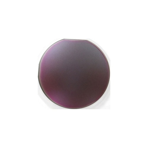
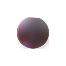
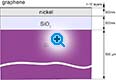
Graphene™ films are grown directly on a Ni/SiO2/Si deposited on an oxidized silicon wafer usinga CVD process.
SPECIFICATIONS : Research Grade , about 90 % useful area
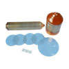
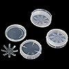
Wafer Size
100 mm diameter
Growth Method
Chemical Vapor Deposition (CVD) Technique
Film thickness : 1-10 monolayer thick
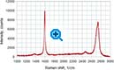
•Graphene film is multilayer with thickness varying in the range 1-10 layers; •Graphene layers are aligned relative to each (graphite-like A-B stacking ) other as indicated by the Raman spectrum •The graphene is grown on Ni film by CVD process. •Nickel film is deposited on the substrate covered by thermally grown oxide layer •Thickness of the Ni layer is 300 nm; •The thickness of the silicon oxide layer is 500 nm; •The thickness of the wafer is 500 m;μ •The crystallographic orientation of silicon is 100;
•films are continuous with low defect density. •Atomically thin carbon film ( 1-10 layer ) •Outstanding electronic properties •Chemical inertness and stability •Unprecedented mechanical strength
Graphene film structure: three film graphene film thickness varis from 1 - 10 layer carbon