GaN Epitxial Template on silicon is made by a hydride vapor phase epitaxy (HVPE)-based method.
During the HVPE process, HCl reacts with molten Ga to form GaCl, which in turn reacts with NH3 to form GaN.
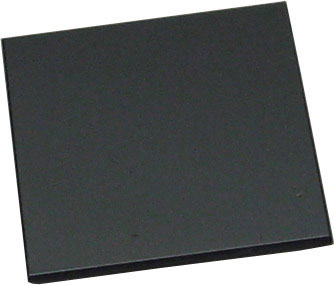
Epi GaN template on silicon is a cost effective way to replace GaN single crystal substrate.
Specifications
Nominal GaN thickness
0.5 μm ± 0.1 μm
Front Surface finish (Ga-face)
< 1 nm RMS, As-grown, Epi-ready
Back surface finish
Silicon ( 111) N-type P-doped R:0-10 ohm.cm
GaN orientation
C-plane (00.1)
Polarity
Ga-face
Conduction Type
Undoped (N-) and resistivities : < 0.05 Ohm-cm
Macro Defect Density
< 1/cm2
Wafer base
•Silicon [111], •10 x 10 x 0.5 mm, •one side polished